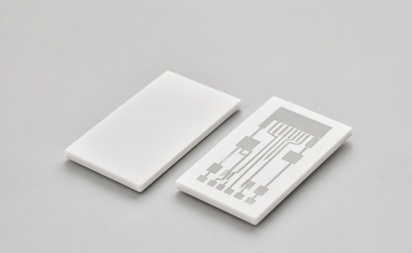
Polished substrates with excellent surface smoothness, tight thickness tolerance and flatness for precision electronics.

Polished substrates with excellent surface smoothness, tight thickness tolerance and flatness for precision electronics.
48H ENGINEERING REVIEW :: NDA ON REQUEST
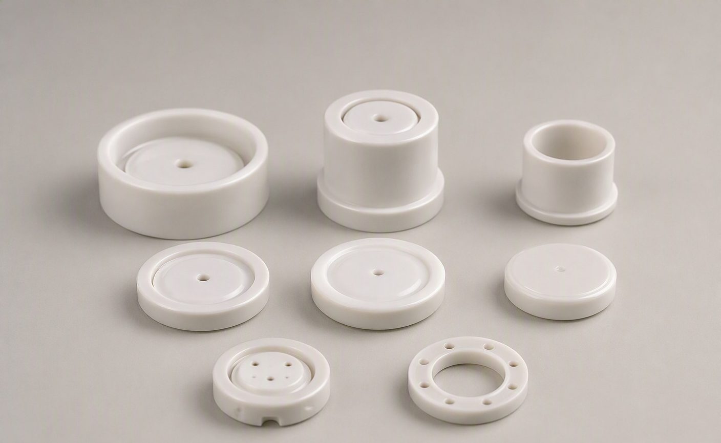
Not sure which grade fits? Our engineers recommend material and tolerance stack based on your operating conditions — media, temperature, pressure and cycle life.
:: Used In| Forming | Dry pressing / isostatic pressing / injection molding |
|---|---|
| Machining | CNC grinding, lapping, polishing, honing |
| Tolerance | Down to ±0.005 mm on ground features |
| Surface Finish | Ra 0.02–0.05 μm lapped · Ra 0.4–0.8 μm as-fired |
| Max Size | Up to Ø600 mm / 800 mm length |
| Prototypes | From 1 pc — no MOQ for sampling |
| Lead Time | Samples 2–4 weeks · production by volume |
Formed and sintered at our Huzhou base, precision-ground in Huizhou. CMM dimensional report, material certificate and optional SEM imagery ship with your order.
Send your drawing through the RFQ form for a documented 48-hour review — or WhatsApp us photos and sketches for a same-day first answer.

High-precision ceramic diaphragms, capsules and bases for pressure sensors — stable from vacuum to high-pressure service.
View Details →
High-strength AlN and alumina substrates compatible with direct copper bonding — the base of reliable power modules.
View Details →
96% alumina thick-film substrates for hybrid circuits — dense, precise and reliable at production scale.
View Details →
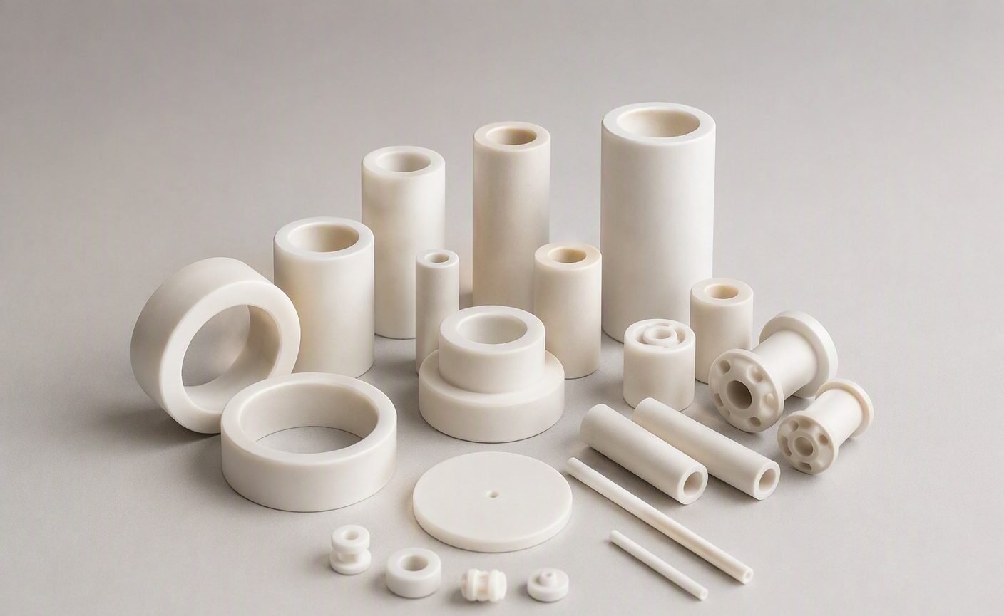
Small pressed and extruded ceramic parts in a wide variety of materials and forming technologies for electronic devices.
View Details →
High-purity alumina thin-film substrates with superior surface smoothness for fine-line circuitry.
View Details →
Glazed alumina substrates with fewer surface voids — ideal for high-resolution thermal printheads.
View Details →
Free DFM review :: NDA on request :: Test data with every shipment